 DLTS is an experimental technique for characterising the electronic properties of deep-level defects in semiconductors. It is the most sensitive spectroscopy yet devised for the detection and characterisation of such defects. The measurement is performed on semiconductor devices that possess a voltage-modulable space charge layer. The most commonly used devices are Schottky-barrier diodes, p-n junction diodes. For a given deep-level defect, the DLTS measurement can, in principle, yield several parameters that characterise the defect and its interaction with free-charge carriers. These parameters include activation energies for emission of charge carriers, cross sections for the capture of free carriers, and the depth distribution of the defect, the last parameter being a property of the material rather than of the defect.
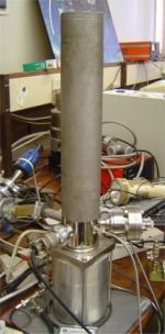
We currently have three DLTS systems. One of them is a conventional lock-in amplifier system while the other two make use of the digital data acquisition card developed by the Copernicus project for Laplace-DLTS. The Laplace-DLTS systems have a much higher resolution and allow one to distinguish close-lying defect energy levels. Two of the helium closed-cycle cryostats can operate in the temperature range 20-370 K, while the third can operate from 12-450 K. We can also do optical DLTS measurements, where instead of using an electrical pulse to excite charge carriers, an optical pulse is used.
 We have two systems that allow us to make automatic IV and CV measurements. These measurements give us an indication of the current transport mechanisms and the free carrier distribution within the depletion layer of the analised material.
One of the measuring stations has a sample holder with a heater. This is used to make variable temperature IV measurements, which allows the Richardson’s constant to be determined for that particular material.
 Carrier concentration and mobility are easily obtained by Hall-effect measurements. Temperature-dependent Hall measurements can further provide information on the carrier compensation ratio, total impurity density, ionization energy, and the dominant scattering mechanism.
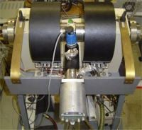
Our setup consists of a closed-cycle helium cryostat mounted in an electromagnet which can generate a homogeneous magnetic field up to 0.6 T. The cryostat allows variable temperature measurements in the range 20-370 K. The system is operated through a Labview program which controls all the measuring instruments which allow complete automatic measurements to be made.
 Knowledge of electrically- or optically-active levels in the bandgap of semiconductors is crucial from both a fundamental physics angle and a purely engineering one. Admittance Spectroscopy is a measurement technique that affords us an opportunity to study these levels and thus gain information on their location in the bandgap and their concentrations. Taken in conjunction with other information, at times, great insights into the nature of these defects could be gained. In contrast to DLTS, Admittance Spectroscopy is particularly attractive as it is not overly sensitive to resistive samples and leaky diodes. Typical applications are the p-type doping studies of GaN. Our Admittance Spectroscopy system can measure either in the Thermal Admittance Spectroscopy (TAS) or the Optical Admittance Spectroscopy (OAS) mode. The range of possible measurements in the TAS system is essentially the same as that accessible through the present “traditional” DLTS system: ET 1eV. Whereas, with the OAS system, defect levels with energies ET about 5eV, could be analysed. And, this enables us to analyse so-called wide bandgap semiconductors, for example, GaN, SiC and ZnO.
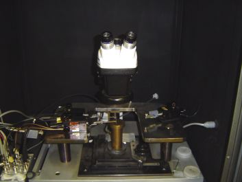
Labview programs control this system. The light source is a 1kW HgXe arc lamp passed through a &14; m monochromator (200 1400 nm). The sample is mounted on a finger in a closed-cycle liquid Helium cryostat capable of operating in the range 15 -370 K. A precision LCR meter is used to monitor sample parameters of interest.
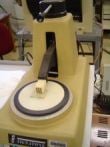 Resistivity measurements are a way of electrically characterising semiconductor wafers, thin films on wafers, and thin near-surface regions of diffused or ion implantation doped wafers. The method of choice for the resistance measurement is the four point probe arrangement of contacts with the surface through which current is passed through the two outer probes and the voltage drop being measured across the inner two. By the use of the appropriate correcting factors and dimensions of the material investigated, the resistivity can be calculated. The resistivity can then also be used to estimate the doping concentration of the material.
Other facilities available to us include the following:
Copyright © University of Pretoria 2025. All rights reserved.


 Virtual Campus
Download the UP Mobile App