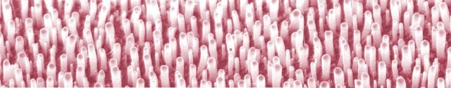
Low-energy bombardment by ions leads to the sputtering of the substrate. Sputtering usually causes a modification of several surface properties. Our studies concentrate on compositional changes due to preferential sputtering and other secondary radiation-induced processes, and on topography development. These surface modifications are not only of fundamental interest in the study of ion-solid interactions, but are also of great importance for ion implantation techniques used in large scale in the semiconductor industry. Topography development due to doping by ion implantation, plasma etching, and various methods of ion beam-assisted metallization can severely affect packing densities of micro-electronic structures. The proper functioning of metal-semiconductor contacts is critically dependent on the interfacial disorder and on compositional changes after ion bombardment processes.
Noble gas sputtering is ubiquitously used in surface analytical techniques for cleaning the surface in situ and for depth profiling. The above discussion shows that sputtering can cause many detrimental affects to surfaces. The results of the above phenomena are employed to develop algorithms for quantitative Auger electron spectroscopy and X-ray photoelectron spectroscopy in the case of sputtering. These algorithms correct some of the detrimental effects of low-energy ion bombardment.
Nitrogen implantation into materials has many technological applications. It is known that nitrogen bombardment of some metals leads to an increase in wear resistance in hardness of these metals. Recently, our group also started working on nitrogen implantation of GaAs, to determine the range profiles of low-energy nitrogen and to determine the composition of the implanted layer. Recently it was discovered that a blue laser can be manufactured from GaN.
Our group has done extensive investigations concerning the effect of ion implantation parameters on topography development, surface disorder and composition. A key aspect of this study has been the close collaboration with a large number of other groups. These included the Chemistry and Geology departments and the Electron Microscope Unit of our Faculty, the Physics department of the University of the Transkei, the research laboratory of TELEKOM at Darmstadt, the Universität Braunschweig and the Max-Planck-Institut für Plasmaforschung in Garching. Results for InP and GaAs have been published in review papers and were reported at several international conferences.
The semiconductor industry in South Africa is focused on Si. The ease of transferring the Si-technology to SiGe makes this compound semiconductor a possible material for future processing in South Africa. We will keep in contact with South African semiconductor device firms such as SAMES to become aware of a possible movement towards SiGe-technology.
Contact: Prof Johan Malherbe
Copyright © University of Pretoria 2025. All rights reserved.


 Virtual Campus
Download the UP Mobile App