At present the group is staffed by the following staff members:
Prof FD Auret
Prof M Diale
Prof WE Meyer
Prof J Nel
Mr M Legodi
Mr J Janse van Rensburg
The group investigates phenomena in several semiconducting materials, including Si, Ge, GaAs, GaN, AlGaN and ZnO. The Group has three main areas of specialization.
Firstly, thin film deposition to form, among others, Schottky and ohmic contacts to semiconductors.
Secondly, we introduce and characterize defects in semiconductors, and evaluate their influence on electronic and opto-electronic devices. The defects are characterized by conventional as well as high-resolution DLTS. The effect of these defects on materials and devices are evaluated by I-V and CV measurements, as well as Hall effect and photo-response measurements. I-V, C-V and Hall effect can be done in the temperature range 10 K – 400 K.
Thirdly, we deposit semiconductor thin films (such as ZnO, NiO and Ge2O3) using chemical methods such as sol-gel spin coating, electrodeposition, chemical bath deposition and spray pyrolysis. These films are then annealed to complete the reaction forming the semiconductor, and then using the techniques described above, the films are analysed with respect to their optical and electronic properties
Defects can be intentionally or unintentionally introduced in the semiconductors. Intentional introduction can be by particle irradiation in our van de Graaff accelerator or by radiation from radio-nuclides. In the case of the van de Graaff it is worth mentioning that the irradiations can be performed in-line at as low as 20 K and then the defects can be directly analyzed by DLTS during the first heat-up cycle. This allows for the study of first generation defects that are normally mobile at room temperature. Unintentional defect introduction includes damage to the semiconductor during some metallization processes. The Group has recently acquired an ICP etcher for controlled etching of electronic materials in an argon plasma and is in the process of acquiring a SPM for electrical measurements on the nano-scale.
The Group has also embarked on a project to fabricate daylight blind UV sensors for several applications. AlGaN is being used for this project which is sponsored by DST.
Germanium has attracted much attention over the last couple of years for its potential use in ultrafast CMOS-devices due to its high electron and hole mobility. Although the most prominent high-energy radiation-induced defects in Ge have been characterized, no in-depth investigations regarding the defects introduced in Ge during critical processing steps, e.g. metallization, have been reported. These investigations are important because it is well known that metallization procedures, e.g. sputtering and electron beam deposition, introduce defects at and close to the metal-semiconductor junction. These defects influence device performance and alter the barrier heights of the contacts. The defects responsible for these barrier adjustments are formed when energetic particles reach the semiconductor surface and interact with the semiconductor. The formation of germanides while annealing at higher temperatures is also being studied, since these can also influence the electronic properties of the material inside the germanide and interface regions.
Click here to see the experimental facilities available in this group.
Click here to see a list of recent publications.
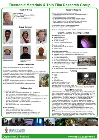
Click on the image to see a poster with more information.

Copyright © University of Pretoria 2025. All rights reserved.
Download the UP Mobile App