

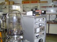
The resistive evaporation system is mainly used to fabricate Schottky contacts on semiconductor materials. Low melting point metals such as Al, Ni, and Au are evaporated in a Bell-jar vacuum system via Joule heating of a crucible containing the material. Deposition thicknesses are monitored by an Inficon thickness monitor.
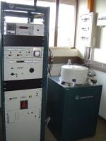
The electron beam deposition system uses a high power focussed electron beam which is scanned over the target material to heat it up. This allows higher melting point metals such as Ti, Pt, Mo, Ru and Cr te be deposited. Depositions are carried out in UHV attained by means of a turbo molecular pump as well as an ion pump.
The system has a sliding target holder, which enables up to four different materials to be loaded and deposited without breaking the vacuum. This is ideal to fabricate Ohmic contacts on semiconductor materials that consists of a layered structure such as for GaN, which consists of layers of Ti, Al, Ni and Au. The interaction of the electron beam with the target, causes the evaporated material to have more kinetic energy. This allows atoms of the first deposited layer to penetrate the semiconductor material slightly, improving the a metal-semiconductor contact with good ohmic properties.
DC & RF Sputtering
In our department we have two sputtering systems, one which is only a DC system and the other a DC and RF system. DC sputtering is used to deposit conducting materials over a sample substrate, mostly just metals.. RF sputtering is used to deposit insulating, conducting or semiconductor materials.
A lot of research was done using the RF system to obtain the optimal parameters for sputter coating of metal surfaces to increase the surface hardness. This was achieved by depositing TiN on the metal surfaces by sputtering Ti targets in a nitrogen atmosphere.
Our RF system is equipped with a specially designed substrate holder which rotate the sample at an angle, around the three magnetrons placed symmetrically around the inside of the vacuum chamber. This allows for very uniform depositions over a substrate surface.
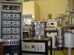
The sputtering systems can also be used in certain semiconductor processes such as surface cleaning or metal depositions.
Our open furnace allows annealing of samples in an inert or reactive gas atmosphere with temperatures up to 1300 K. We typically use nitrogen and argon in this system. Annealing is an important step after deposition of ohmic contacts. This causes the first layer to diffuse slightly into the semiconductor surface and also increase the adhesion between the deposited layers onto the semiconductor.
The vacuum furnace is used to anneal samples under vacuum or small controllable amounts of reactive gases such as hydrogen. Samples are loaded in the quarts tube and pumped down to a pressure of 10-7 mBarr. The furnace can be operated at temperatures of up to 1400 K. It also allows programming of custom made annealing cycles.
Copyright © University of Pretoria 2024. All rights reserved.
 Virtual Campus
Download the UP Mobile App